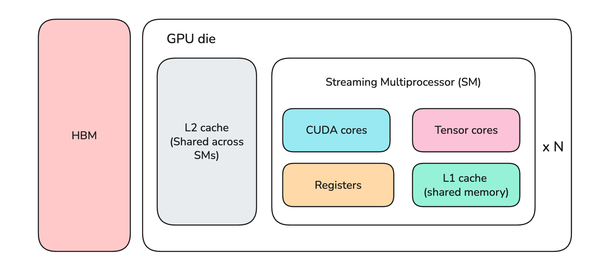

“This is the lesson that you need if you are new to GPUs and want to master them without getting overwhelmed.”
Frameworks like PyTorch are easy to use because they hide away all the intricacies that occur at the GPU level. But companies and research labs today are looking for engineers who can look under the hood of PyTorch, explain where their compute budget is being spent, debug GPUs, and make LLMs more performant.
Here are 9 concepts explained simply that will help you better understand GPUs.
1, 2, 3: discuss GPU computation hardware
4, 5, 6: discuss GPU memory
7, 8: discuss how programs are executed on GPUs
9: discusses how multiple GPUs are connected together
Let’s begin!
1. Streaming Multiprocessor
Streaming Multiprocessor (SM) is the core computational unit in NVIDIA GPUs.
It is similar to the cores of a CPU, with one major difference: it can execute parallel instructions and specific operations, such as matrix multiplication, much faster.
While a CPU core is optimized for high execution speed of a single thread, an SM on a GPU is optimized for high throughput across many threads (running a large number of threads in parallel).
A Streaming Multiprocessor (SM) is called so because:
It works with streams of data (data inputs requiring similar computation that are continuously fed to it)
It contains multiple processing units that can perform computations on a data stream in parallel
The main components of an SM are:
CUDA cores (INT32, FP32, FP64): For basic arithmetic calculations
Tensor Cores: For matrix multiplication calculations
Warp schedulers and Dispatch units: For choosing which thread groups (warps) to run next
Load/ Store (LD/ST) units: For moving data between memory and registers
Registers/ Register files: For storing each thread’s data temporarily
L1 cache: For temporarily storing data to be used across the components of an SM
Shared memory: Partition of the same SRAM as the L1 cache that can be used to store data. While L1 caches data automatically, shared memory can be used programmatically.
The following is an architectural diagram of the SM for an NVIDIA H100 GPU. A single H100 SXM has 132 such SMs.
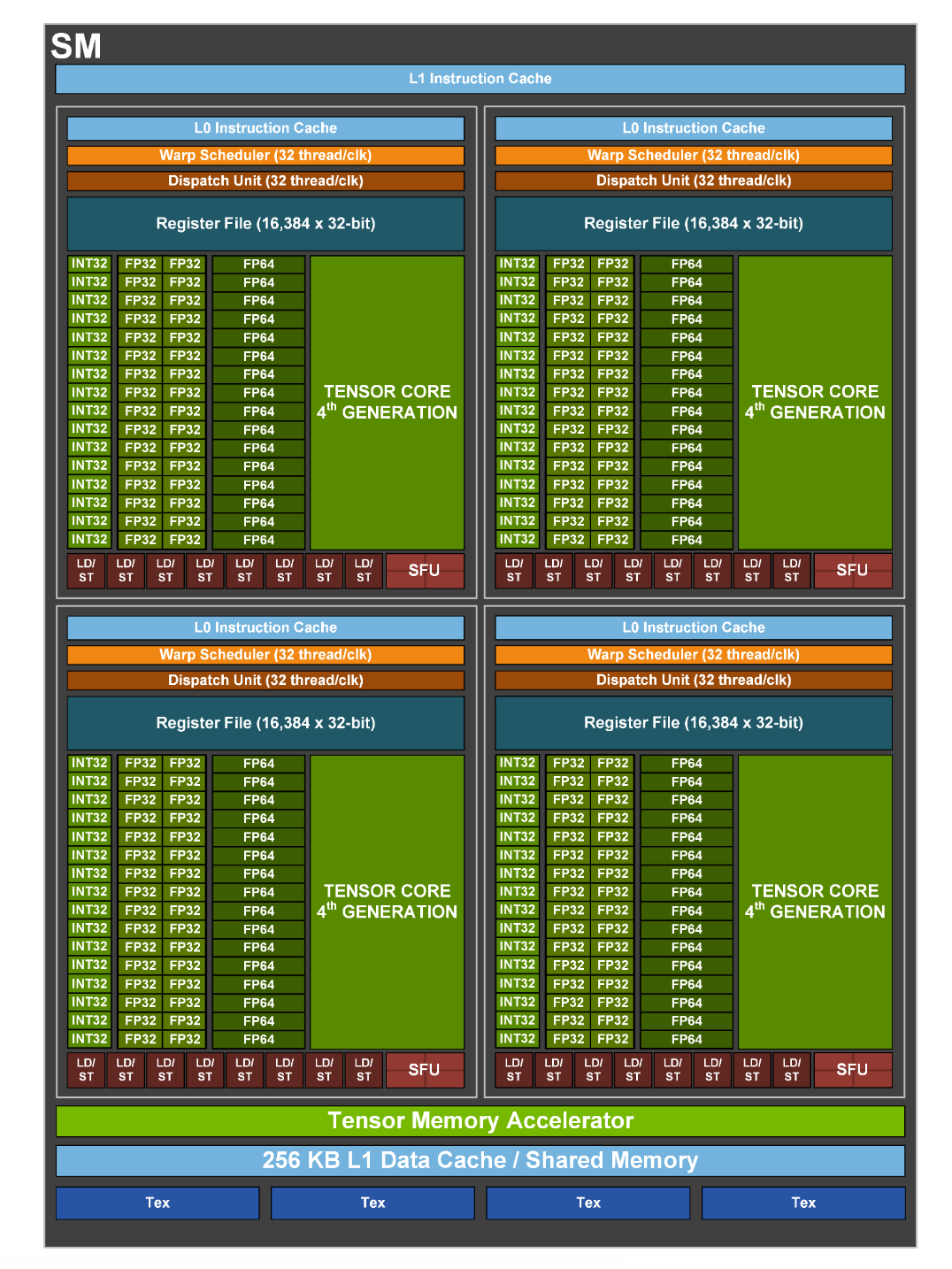
Although the above-mentioned components are most common in GPUs, you can see many more components in the H100 GPU, such as:
SFUs (Special Function Units): For performing exponential, logarithmic, and trigonometric functions.
Texture (Tex) units: For processing surface texture data efficiently
Tensor Memory Accelerator: For efficiently moving multi-dimensional data between global memory and shared memory
L0 and L1 instruction cache: Small and fast cache memory that stores frequently used instructions close to the compute cores
2. CUDA core
A CUDA (Compute Unified Device Architecture) core handles a single simple arithmetic operation, such as integer and floating-point calculations, per clock cycle, in an SM.
Different CUDA cores handle different types of numerical precision, such as INT32, FP32, and FP64, as seen in the architectural diagram above.
An H100 SXM GPU has:
128 FP32 CUDA cores per SM
16,896 FP32 CUDA cores per GPU
A CUDA core is much simpler than a CPU core. While a CPU core can perform complex operations, a CUDA core’s job is to work as a simple calculator for basic arithmetic. It is the massive number of these cores performing calculations in parallel that makes a GPU so powerful.
Note that the term ‘CUDA core’ refers to hardware and is not directly related to the CUDA software ecosystem.
3. Tensor core
A Tensor core is a specialized unit in an SM that can perform fast matrix multiply-and-accumulate operations.
These operations make up the bulk of the workload in deep learning and are handled by the Tensor Cores, leaving non-matrix operations (such as activation functions, normalization, and element-wise operations) to the CUDA cores.
NVIDIA first introduced the Tensor Core in the Volta GPU architecture in 2017, which massively accelerated neural-network training workflows.
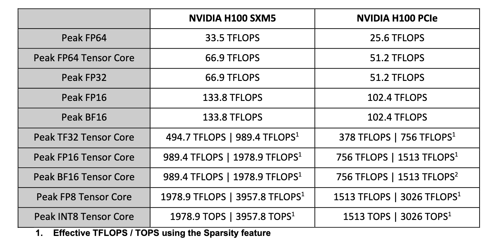
Tensor Cores are also specialized for different numeric precisions, such as FP16, BF16, TF32, and FP64. The H100 GPU has specialized tensor cores for low-precision formats such as FP8, while the Blackwell generation of GPUs includes tensor cores for FP4 (specifically, NVFP4).
You will often find discussions of TFLOPS in GPU specs, which refer to the performance of the GPU's Tensor cores and CUDA cores.
4. High Bandwidth Memory
High Bandwidth Memory (HBM) is a GPU’s main memory. It is also called global memory or VRAM. This is the memory that holds the model weights, activations, and KV cache.
HBM is mounted alongside the GPU die and works with smaller memory components (L2, L1, and register files) that are etched directly on the die (on-chip memory).
It is a type of Dynamic random-access memory (DRAM), which offers larger capacity and is cheaper than on-chip memory, a type of Static random-access memory (SRAM), which is extremely fast but much smaller.